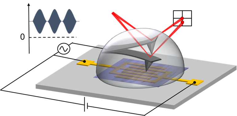
Schematic representation of the in-liquid Scanning Dielectric Microscopy set-up used to measure the local electric properties of an electrolyte gated organic field effect transistor (EGOFET) under operation. The sharp electrode tip mounted on the cantilever sensor can sense the local electric forces at the semiconductor/electrolyte interface when MHz frequencies are used.
Electronic biosensors based on organic materials are currently evolving at a very fast rate. Organic bioelectronic devices like the Electrolyte Gated Organic Field Effect Transistor (EGOFET) or the Organic Electrochemical Transistor (OECT) can make soon a reality the dream of low-cost, disposable, flexible and biocompatible electronic devices for the interaction with biological systems. Applications based on these transistors such as implantable organic biosensors to record the electrical activity of neurons in in-vivo conditions or the development of prosthetic electronic skins based on organic biosensors are already a reality in research labs and offer great promises for medical applications in the near future.
Microscopy based on electrical forces for the optimization of organic devices operated in electrolyte solutions
Still, bringing these devices from research labs to the market requires further optimization. The development of many of these devices is currently hampered by the difficulty in visualizing the electrical and electrochemical processes occurring at the interface between the biosensor, the liquid solution and the biological system of interest at the very small scales (the nanoscale). In this study, an important step towards solving this long-lasting issue has been given. Specifically, it has been shown that the conductivity and interfacial capacitance of organic biosensor/electrolyte interfaces can be mapped with nanoscale spatial resolution in an organic biosensor under full operation conditions. To achieve it, a microscopy technique developed some years ago in the Nanoscale Bioelectrical Characterization group at IBEC lead by University of Barcelona´s Professor Gabriel Gomila has been key. This technique, referred to as in-liquid Scanning Dielectric Microscopy, can probe the electrical properties of solid/electrolyte interfaces by measuring the electric force between a very sharp tip mounted on a microscopic cantilever and the biosensor surface.

To get rid of the screening and dissipating effects produced by the liquid solutions with ions, frequencies in the MegaHertz range are used. Measuring electric forces rather than electric currents, as other techniques do, provides unparalleled sensitivity and spatial resolution to in-liquid Scanning Dielectric Force Microscopy. In the present work, it has been imaged for the first time how electric charges accumulate at the biosensor/electrolyte interface when an external (gate) voltage is applied to an operational EGOFET and how a nanostructured ultrathin insulating layer just a few atoms thick is present at its surface and determines the device performance. The EGOFET analyzed in this study was developed in the group of Dr. Marta Mas Torrents at ICMAB and it has the capability to record the bioelectrical activity of electrical excitable cells.
This study, by visualizing electrical properties of biosensor interfaces that until now had remained invisible, offers novel avenues for the optimization of the performance of the organic biosensor devices and paves the way for its faster adoption in applications in the medical real.
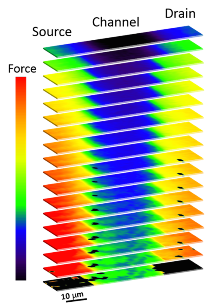
Figure: Electric force images acquired at decreasing distances from the channel of an electrolyte gated organic field effect transistor (EGOFET) under operation. At the closest distances (bottom) the heterogeneous nanoscale electrical properties of the channel emerge and become visible and measurable.
Reference article: Adrica Kyndiah, Martí Checa, Francesca Leonardi, Ruben Millan‐Solsona, Martina Di Muzio, Shubham Tanwar, Laura Fumagalli,Marta Mas‐Torrent,Gabriel Gomila. Nanoscale Mapping of the Conductivity and Interfacial Capacitance of an Electrolyte‐Gated Organic Field‐Effect Transistor under Operation. Advanced Functional Materials, 2020.


