
A study led by IBEC has successfully mapped the local electrical potential along the structure of organic transistors used in bioelectronics, enabling a detailed assessment of bottlenecks in charge transport. The goal of this study is to deepen the understanding of the properties of charge transport in materials used in organic electronics when in contact with liquid media, aiming to enhance their applications in biosensors or bioelectrical recordings.
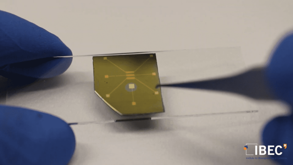
Electrolyte gated organic field-effect transistors, known as EGOFETs, have gained significance in recent years as fundamental components in bioelectronics. These electronic devices can convert biological and biochemical inputs into amplified electrical signals while operating in aqueous environments. Moreover, they are fabricated with organic semiconductor materials, making this technology more biocompatible, flexible, and cost-effective compared to conventional silicon technology.
However, organic semiconductor materials consist of various crystals with imperfections that can impact the transistor’s operation. The ability to employ nanoscale analysis techniques for a detailed study of how these imperfections affect the transistor’s operation is crucial in the quest for creating more efficient and reliable devices.
The major innovation of this work is the ability to create potential maps while the material is in contact with an aqueous medium without short-circuiting it.
Shubham Tanwar
Now, a study led by IBEC’s Nanoscale bioelectrical characterization group has successfully developed a methodology capable of mapping the local electrical potential along the structure of EGOFET transistors while they are in operation. This initiative allows for a detailed assessment of bottlenecks in charge transport. The results obtained have the potential to deepen the understanding of how the structure of the material affects its properties and functionality, providing new paths for optimizing device operation and ultimately enhancing its applications as biosensors or bioelectrical recording instruments.
“The major innovation of this work is the ability to create potential maps while the material is in contact with an aqueous medium without short-circuiting it,” says Shubham Tanwar, a recent PhD graduate from IBEC and the first author of the study.
“From the measurements made, we have observed that when a voltage is applied, most of it, instead of moving the electrons, is deflected to the areas where two different crystals are in contact or in the electrical contacts,” says Dr. Adrica Kyndiah of the Italian Institute of Technology, who co-led the work. “This technique allows us to obtain additional information without performing complicated calculations, simply by intelligently manipulating the experimental data. From here, we can address various problems related to the materials,” explains Gabriel Gomila professor at the University of Barcelona and principal investigator at IBEC, who co-led the work.
The new approach, which is already available to professionals in the field, has sparked interest from international groups, with whom Dr. Gomila’s team is establishing collaborations to analyze their own devices. In addition, the possibility of integrating artificial intelligence to further automate the procedure is being explored.
The study has had the collaboration of the Italian Institute of Technology and Dr. Marta Mas-Torrent research’s group at the Institute of Materials Science of Barcelona (ICMAB-CSIC).
Referenced article:
Shubham Tanwar, Rubén Millán-Solsona, Sara Ruiz-Molina, Marta Mas-Torrent, Adrica Kyndiah, and Gabriel Gomila. Nanoscale operando characterization of electrolyte-gated organic field-effect transistors reveals charge transport bottlenecks. Advanced Materials (2023). DOI: 10.1002/adma.202309767


